On board of my boat I have a 12V system. To charge the laptop while on the water you can use a 12 to 230V sinewave inverter but it would be efficiënter to go from 12V direct to 19 via a boost converter.
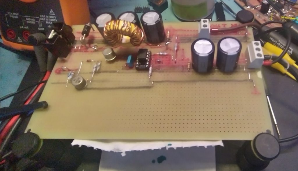
This one I build using an oldie but goldie, the 34063. But I needed 2.5A and this IC is limited to 1.5A. To solve that the datasheet extends the schematic with an external transistor. But to get a better rendement I wanted to use a MOSFET. This because the biggest part of the waisted power is in the “switch” (the transistor or MOSFET) The MOSFET I chose for the first test setup was a beefy one, capable of passing a lot of current. Mounted on a little heatsink it became pretty hot. The efficiency was bad. All that current heating up the MOSFET was waisted in heat.
The principle is you short a coil to ground (via the conducting MOSFET) , current runs through it, you open the switch (turn off MOSFET) and the energy in the coil flows via the diode to the load. While shorting the coil you want as less resistance in the switch as possible. That is called the Rds-on, the resistance of the drain sourse channel if the MOSFET is on. The first MOSFET that got so hot had a 1 ohm resistance. The final version uses a FQP65N06 and has a resistance of only 0.016 ohm.
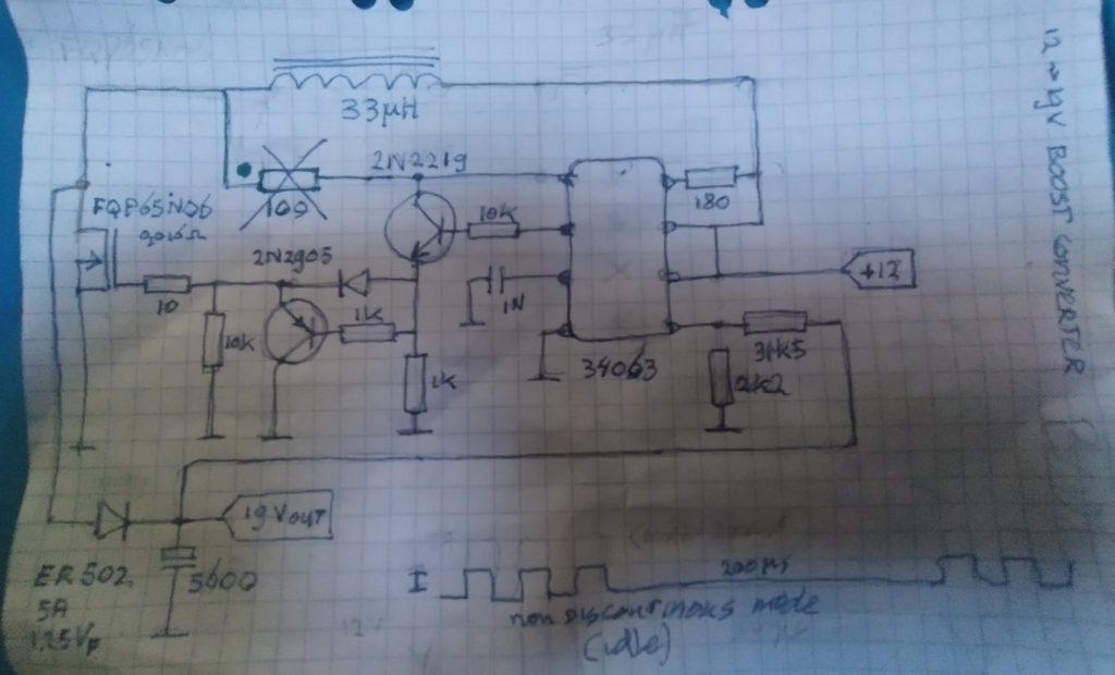
But you want that MOSFET to switch on and off fast because that 0.016 only counts if it is fully switched on. The gate is a capacitor so the voltage follows the current and this causes a delay, discharging it also takes time. The first huge MOSFET got extremely hot. To help that speed up I added 2 transistors. This for most helps to discharge the gate and so the fall tim becomes a lot shorter. I had troubles getting it to work until I removed the 100 ohm resistor connection. This should be needed because pin 1 is an open collector (according the datasheet) I removed it to measure some things because it would not work. To my supprise it then worked. The efficiency was better, the MOSFET only got hot but not to hot. To get that cooler I needed less channel resistance and switched over to the 0.016 ohm version. That solved the poor efficiency.
But there is an other difficult thing building a switcher, the coil. For a SMPS inductor you need a core with a low Al because the higher the Al, the more energy will be stored in the core instead of in the coil itself. The best shape is a toroid, the best Al is 1 (= 1 nH/turns squared) and that is air. So I tried a core with a higher Al and cut out an air- gap. This worked but was noisy. I think the material reacting to the magnetic field modulates the air. The disadvantage of a low Al is that you need more turns, and that is more copper is more resistance. So you need to find a compromise.
The datasheet and books about switchers give you formulas to calculate the self-inductance. This is harder as it looks due to the data you need. You can do it by trial and error but an IC like this will work with almost every self-inductance. However, the losses in the core-material and copper is waisted energy and if the core saturates the self-inductance becomes very low (the Al becomes 1) and current increases a lot and things can go south fast. I followed the formulas and calculated 33 uH. The timing cap 1nF. De cores Al = 62nH/n2. No clue what type of material. Most important, It does not saturate at 2.5A
Routing and layout is important because the peak currents are high and the converter can radiate a lot of EMI. I used per rail 3 strips tinned and interconnected. 2 times 3 strips for ground, one for 12V and one for 19V. They all run straight from left to right. So the biggest currents run via a straight low impedance path.
At no load the controller runs at non-continuous mode. As current increases the controller goes in to continues mode.
Without a load so every now and then a few groups of pulses appear on the gate. They vary in duty cycle. The converter draws a few mA. The shape of the gate voltage during rise is not great but it switches off pretty fast.
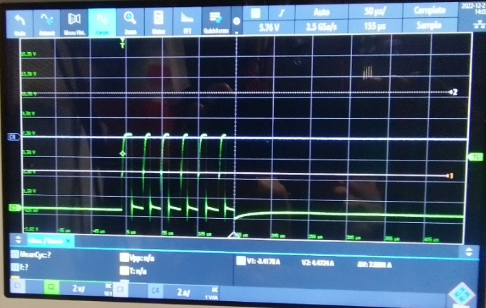
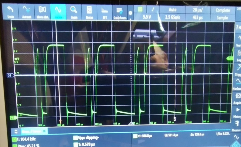
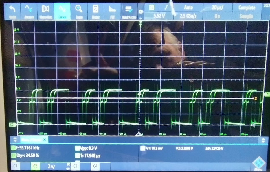
At 100 mA the pulses appear no longer random. The time between the groups varies also a little but most are about 1 ms apart. Still in discontinues mode. This all is with a 12.5V input. The input power is 2.41W and the output is 1.98W. So we loose about 0.4W.
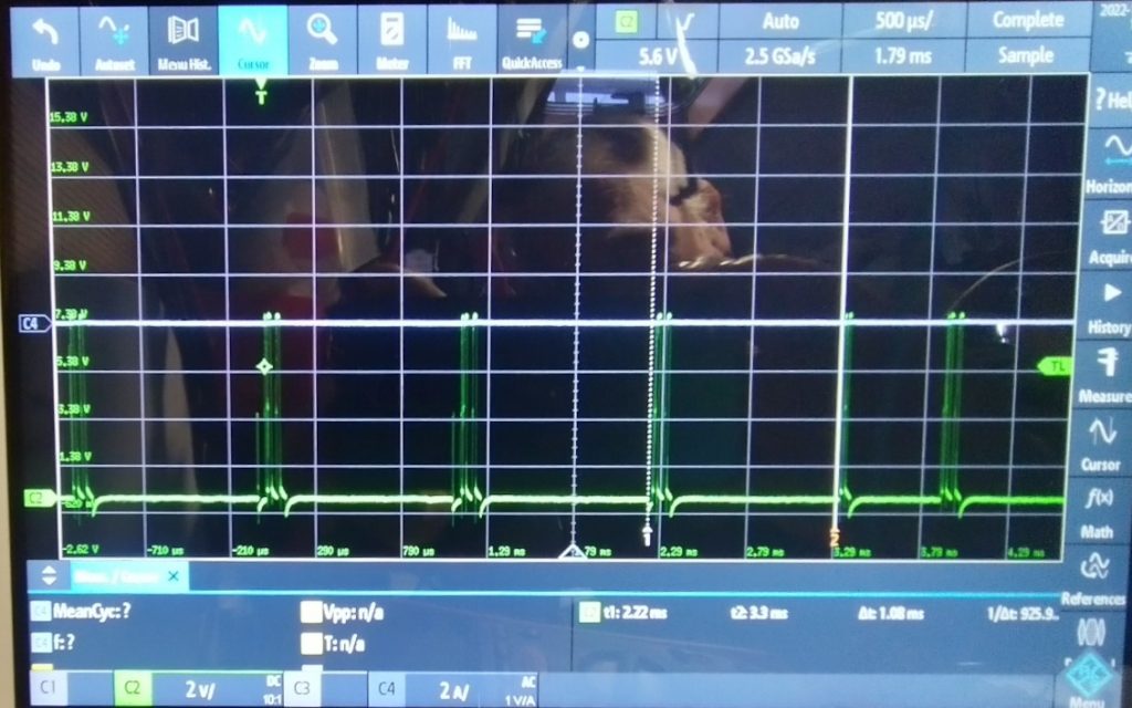
At 500 mA still in discontinuous mode. The time betyween groups is decreased to 200 uS. output is 9.66W, input 11.82W
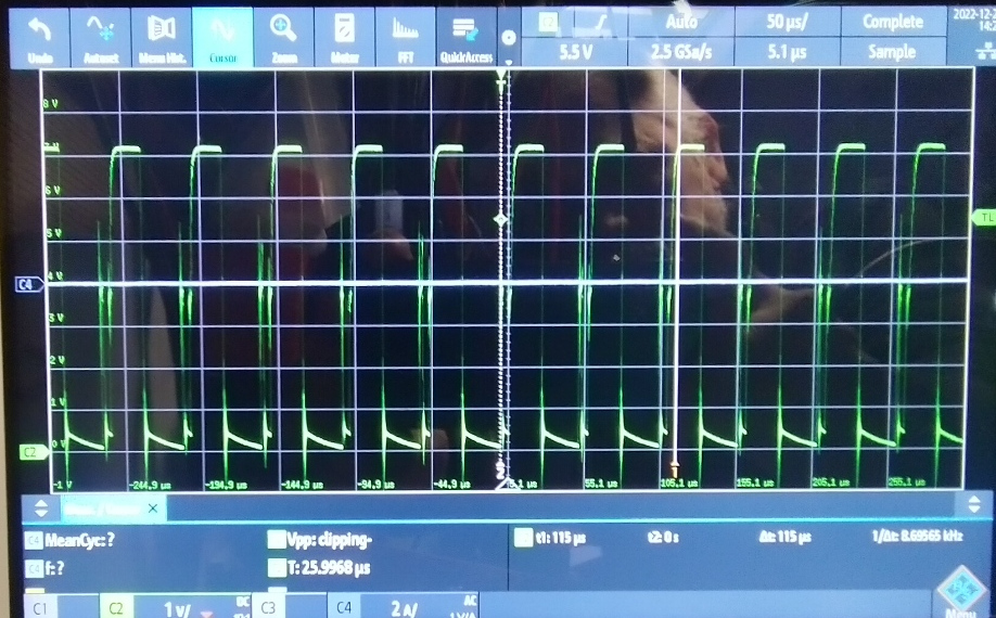
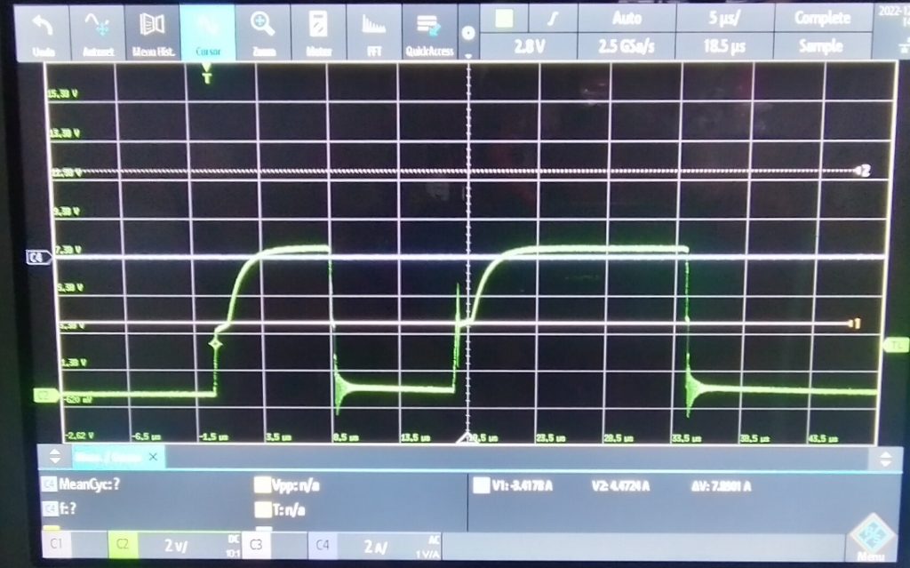
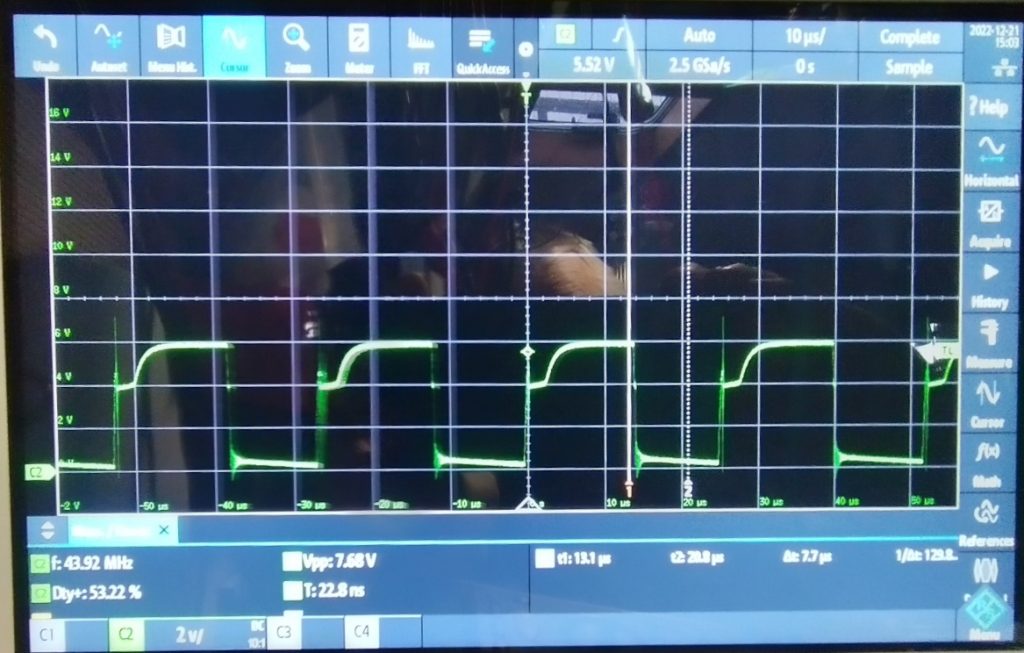
Now it runs in continuous mode. Input is 24.18W, output is 19.24W. one pulse takes 22 us and +41% dutycycle. This varies a bit. The gate is not perfect. There first is a very short puls before the main pulse. Gate voltage is in all situations around 9V. The signal on pin 1, the “open collector” is 8Vp so I do not think it really is open collector. I only buy parts via companbies as Farnell and Mouser but these ICs are from my own stock, I have them over 10 years so I do not think they are fake or so. Maybe the IC is changed and I used the wrong datasheet. The components still are cool to touch.
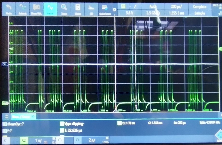
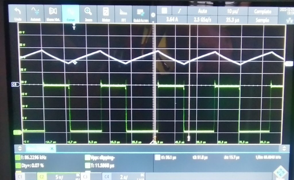
Same as 1A but now 28.83W output and 36.42W input. The longest pulses are 20 us. Input current is nice and flat so the powersupply (10A Delta) has no problems supplying the converter.
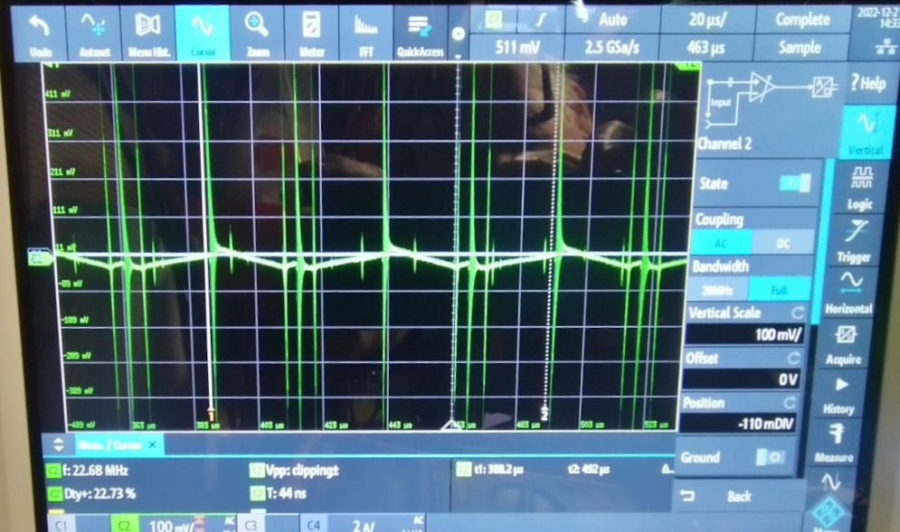
The output ripple at 1.5A is around 50mVpp and a lot of grass on it. There is no filtering other then the output capacitance. But SMPSs spray a lot of EMI around so it is possible the probe picks that up to. The next step will be a filter. If you use a metal case and a filter SMPSs can be very clean.
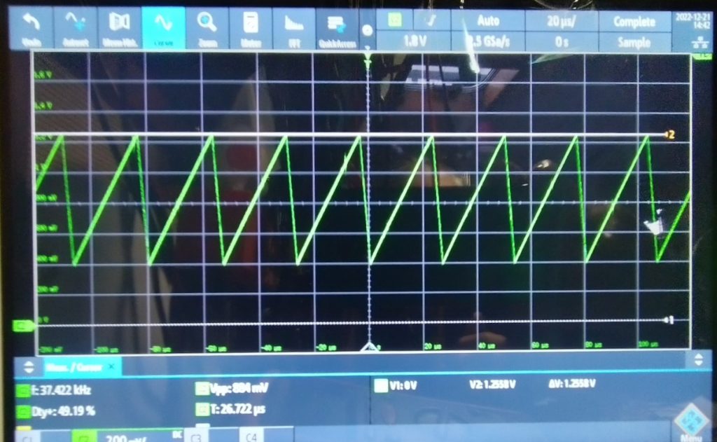
The frequency is set by the capacitor on pin 3. I used a 1 nF and the frequency is 37.4 kHz. This is a stable frequency. Vpp is 880mV
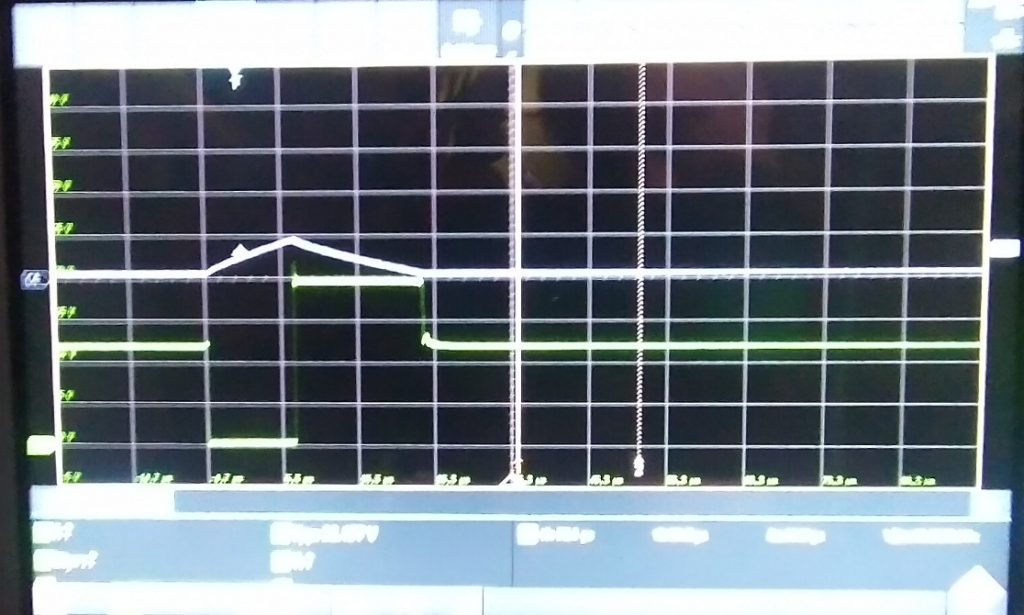
At 2A the input is 49.96W. The output is 38.42W. I do not know if the powermeter can handle the EMI. Looking with a current probe the input current is clean so the input capacitance is big enough and the PSU has also no problems.
Something strange happens. The gate starts a few seconds like above (only 6Vp) and then switches to 9Vp. Another strange thing is that I will deliver almost 3A before the output voltage collapses but It will not start if the initial current during connection goes over 2.1A. No clue why. At 2.5 the inductor becomes warm and the mosfet gets a bit hot. I must do some more tests to watch the temp over time. I probably will end up with a bigger heatsink. The dutycycle is now 53% and it needs 63.7W to produce 46.7W. so only 73%. That is not great. But it is a charger I will not use often.
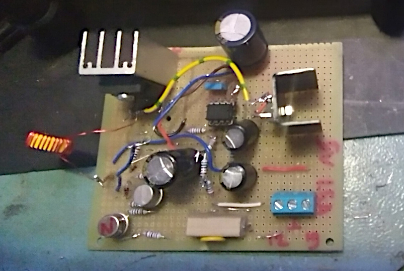
Update, I placed a bigger heatsink. replaced the inductor for a bigger diameter core, thicker wire, Al=87, n=22, 42uH. I added a filter. Series inductor is 2.7 mH and parallel C is 2200uF. Now the output is clean, ripple even smaller and now the converter starts up fine under full load (2.5A). And as a bonus, 45,9W output needs 58.1W input, giving now 80% efficiency under full load.
Update 2: The MOSFET died during further tests (He refused to start up at full load if the input voltage was 11.78V. I now replaced it with a IRLZ24, a logic level MOSFET. Now the drain voltages shows a near perfect squarewave. Also no startup problems at lower voltages (Goes well down too 10.8V). Now add some protection etc like a fuse, power-on led, MOV, zener for the gate etc.
Update. I think there was something wrong with the smps controller in my test/measure version. Because I can hook pin 1 to the powersupply in the definitive version (via a resistor) without killing things. But it has no noticeable effect on the gate voltage or drain current. No clue why. If it really is open collector there flows current from the internal open collector transistor via the diode connection out of pin 2. The same for the 2n221`9. The IC can handle those small currents and the mosfet goes full open at 5V.
I tried an other driver, also 2 transistors but now a bit like a half bridge. The top npn switches the MOSFET full open if pin 21 is high, the pnp is not conducting. If pin 2 gets low, the npn stops conducting and the pnp switches on and pulls the gate to ground. This probably works better for a normal MOSFET but was no improvement with the logic MOSFET.