
Vackar met twee BFR93 torren
September 2011: This will be a long time project. First plan was to make the CO’s myself.
This one is made on pcb. First at 5V but later 12V. I could not get it to run from 500MHz to 1Ghz with one oscillator. The cause seems to be the BB535 varicap.

A vackar oscillator, Here without varicap. The red wire is the coil.
I also tied it the lassic way. I used a BFY90. This has only a Ft of 1.5GHz. It ran without problems from 500-1000 but not within the range of the varicap.

.dead bug vackar, de grote spoel is de RFC
Time to try the good old wunderhorn. A negative resistance oscillator . The name and design is from FAS Sterrenburg. I have made this one using tubes, FETs, and transistors. It alway worked great. Builded versions from 1 MHz upto 1GHz. But here the same problem.

Aangepaste wunderhorn
To get high enough in frequency you need enough Ic, if that gets to low the Ft of the transistor decreases.. The wunderhorn uses a 1 to 2K emitter resistor to do this. The schematic is a pricipe I used for the tests. The definitive version uses other values.

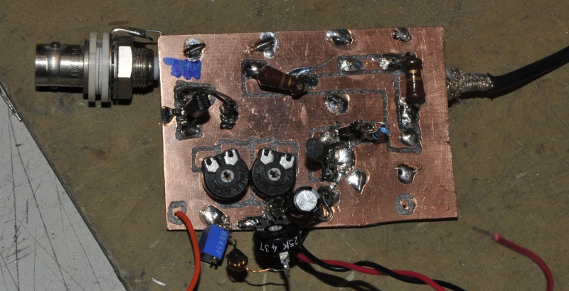
Wunderhorn, de twee torren verzonken in de pcb

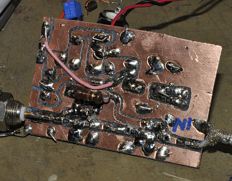
van opzij, een mix van smd en klassiek
After enough problems I decided to use a VCO’s developer kit from minicircuits

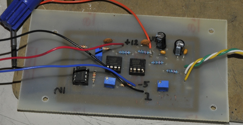
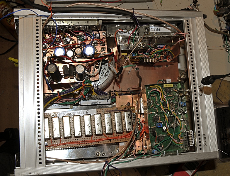
De voeding met alle rails
The powersypply, 24V, 12V, 8V, 5V and -24, -12, -5V
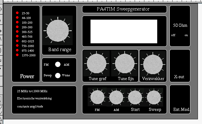
The sweepgenerator. 0-5V, adjustable sweep and offset. Also a LT1027 Vref and opamps that make 0-20 and 0-15V Vtune. The other pcb is a low distortion 1 kHz sinus generator for AM modulation.

Vtune, Vref en modulatie
First trial. To much space ande instable mounting.

een van de tien VCO boards, filterkant

VCO board kant met een van de 10 mini circuits POS VCO’s

De twee backplanes met voedingslijnen
This was the setup as planned at first. The pCBs were to wobbely and it took to much space.

Powersupply filter board
New approach. I like dead bug more as making 10 pcb’s.

The 25-50 MHz VCO

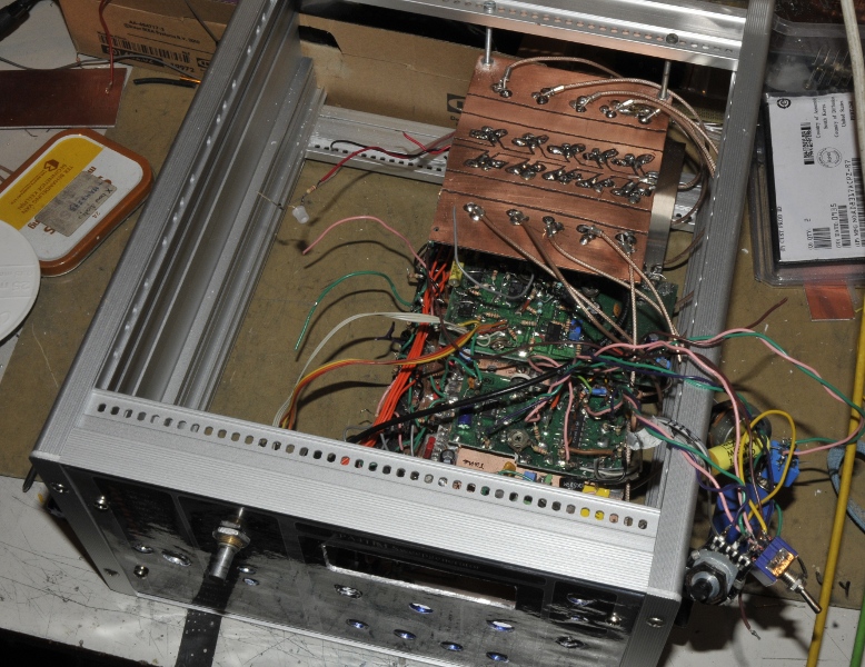
The box that holds all filters and VCOs

Temporary frontpanel, VCO’s and filters.
The blue boxes are relais that switch on the VCO’s, a led and Vtune. The first filters are lumped, The last 2 microstrip, The others a mix of microstrip and lumped. All tested with the SDR VNWA.
Juni 2012:
To much crosstalk so I changed relais operation. Now only one VCO is switched on when choosen. The output is allmost +10dBm.
Everything works. The next step will be the pinattenuator, controller, powermeter, RF relaisboard and Frequency/powermeter reading .

Overzicht

De filters
De hoogste filters. De laatste twee zijn microstrip. De twee daarvoor zijn eigenlijk niet echt definieerbaar. Het is een stripline achtig idee maar dat is het niet. De rechtopstaande stukjes pcb zijn condensators welke met stukjes draad zijn verbonden. Soms ivm betere afscheiding tussen de trappen met een bochtje. Erg makkelijk te maken. Je berekent het oppervlak soldeert hem op zijn plaatst. Sluit een C meter aan en vijlt hem op de juiste waarde. De spoeltjes maak ik op de zelfde manier. Het resultaat is een filter wat nagenoeg in een keer goed is. Er voor zitten de VCO’s van minicircuits. Erg mooie dingen. Voor dit project heb ik de development kit besteld. Dat is een stuk goedkoper dan losse VCO’s.

The PSU, a bit overdone

De POS100 start frequency

POS100 end frequency
All filters are like this and some even better.
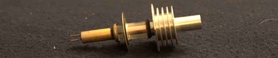
The powermeter based on a AD8317. This will measure the output power and control the pindiode attenuater based AVC.
AD8317 powermeter
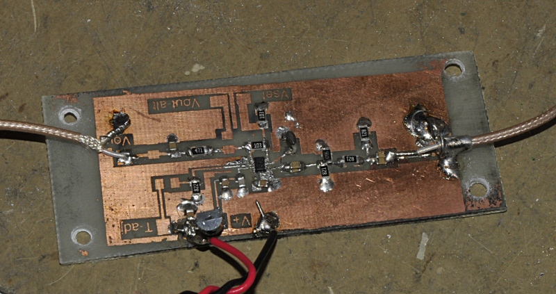
Powermeter PCB
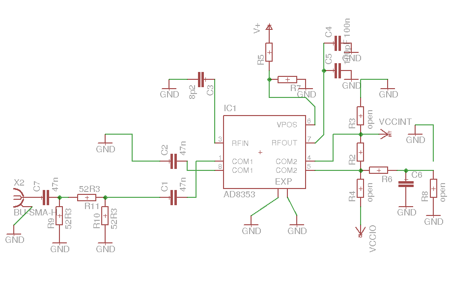
Schematic (fbased on AD datasheet)
The output from the powermeter goes to the controller that makes a signal to control the pindiodes to keep a constant amplitude and control it manual too.
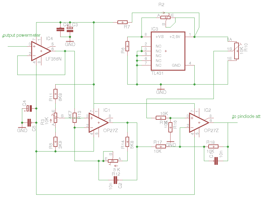
amplitude control
controller
controller
pindiode attenuator
This is just the principal schematic. The 4 1n4148 diodes are smd pindiodes and not all values are correct. I used this as a starterpoint. The attenuation range is 0-30 dB
pin attenuator top
pin attenuator underside
I used Xfig to design the front
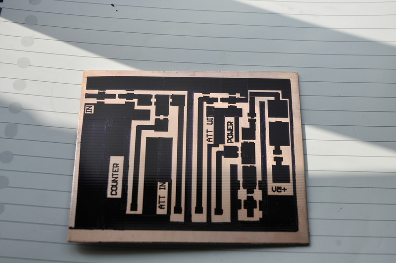
The relais board to connect VCOs to powermeter and attenuator
Underside board
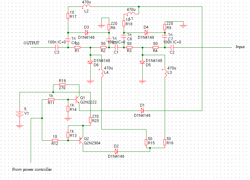
Just plotted splitter-amplifier board
The powermeter, counter, AVC controler, relaisboard etc come together on this board. I make boards by using a HP penplotter. I modifoed a CD marker and fill this with edding 3000 ink. Works very good. If you look good you see in the right upper corner you see to very thin lines. They are almost as thin as a knife cut. The plotter managed to draw this the right way. This is for a 15 dB AVT50663 gainblock with 6 pins and smaller about as big as a 0806 resistor.
Schematic splitter:
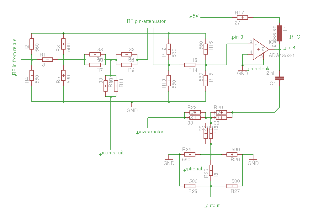
Splitter schematic, the gainblocktype is only chosen for the footprint.
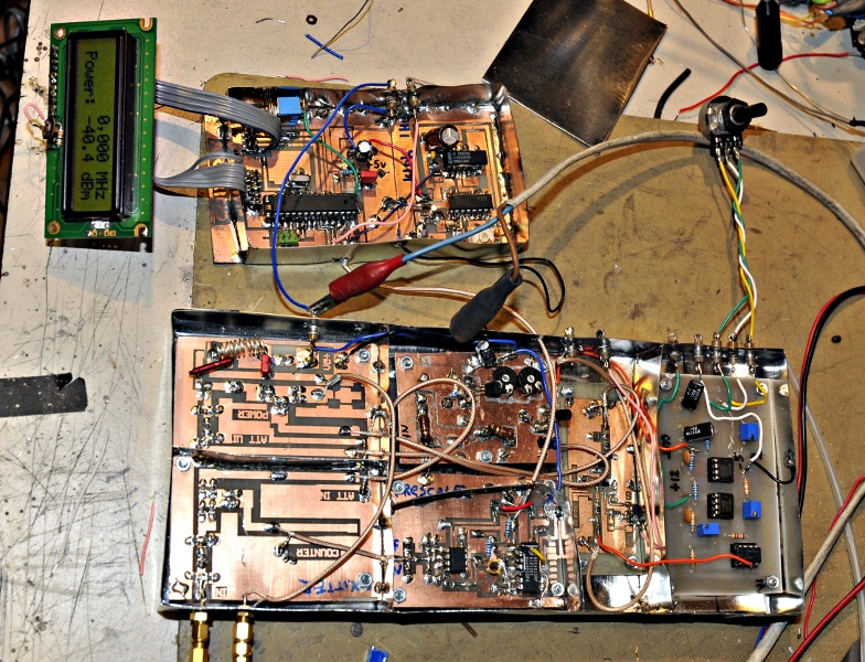
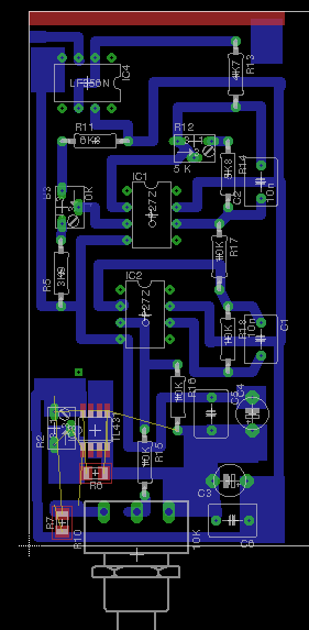
Power control and read-out
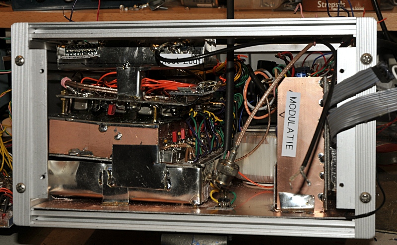
Everything mounted in a tinbox, here still without the cover.
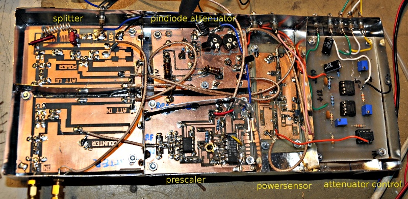
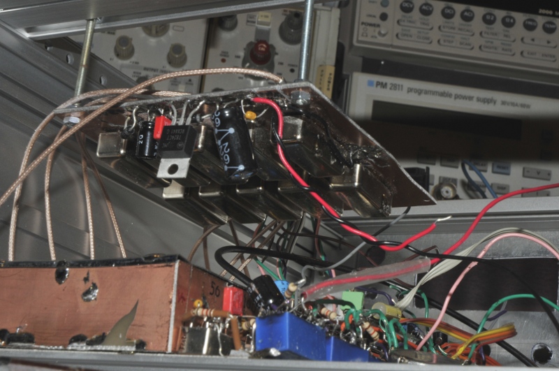
Pindiode attenuator and powercontrol, powermeter, prescaler and splitter.
Most right the powercontroller tyhat reads the powersensor and keeps power level at a value that is set with a potentiometer at the front by biasing the pindiodes. It gets the power from the AD8317 sensor that is the pcb left of it. Then the 2 GHz (devide by 512) prescaler. Above that the pindiode attenuator. They are smd and mounted under the pcb. Most left isthe splitter. RF power from the relaisboard enters gere through the left smb connector. It is then attenuated 3 dB to get a good powermatch. The performance of the filter depends on a good match. Then a splitter splits the signal to the pindiode attenuator and to the prescaler.
After the pindiode attenuator the signal enters the board again and an other power splitter connects it to the powermeter and the smb output connector that will go to a bnc on the frontpanel. The powermeter output and prescaler output go to the Arduino based counter and powermeter (with a 1Hz gate generator) The powermeter output also goes to the attenuator controller.
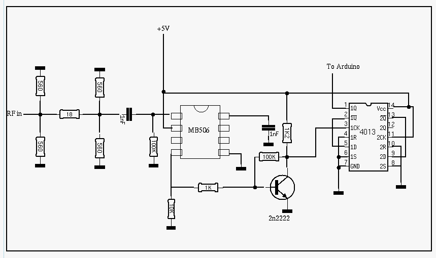
The counter is not the usual arduino way using the frequency.h lib. It is independend of the Atmel clock (it runs at 12 MHz insteda of 16 MHz in this case). The 1Hz ( 1000,000.0 ms period time) generator based on a watch Xtal, 4060 and 4013 is the timeperiode the Atmel starts counting. This is limmited to 10 digits because of the max size of the variable but that is more then perfect for my use. A test without the prescaler and a 1,000.000 MHz testsignal gave a 512,000.003 MHz reading on the display. So it is only 3 Hz off at 512 MHz. That is way below 1 ppm . The software is for the main part written by Pros, a Circuits online member. Thanks Pros (his nice website : http://prosje.be/index.html )
Down here you find a downloadable pdf file with the Arduinocode:
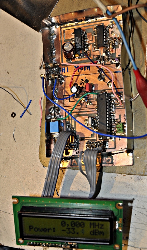
Arduino programmerd ATmega328 based counter and a 1Hz gate generator
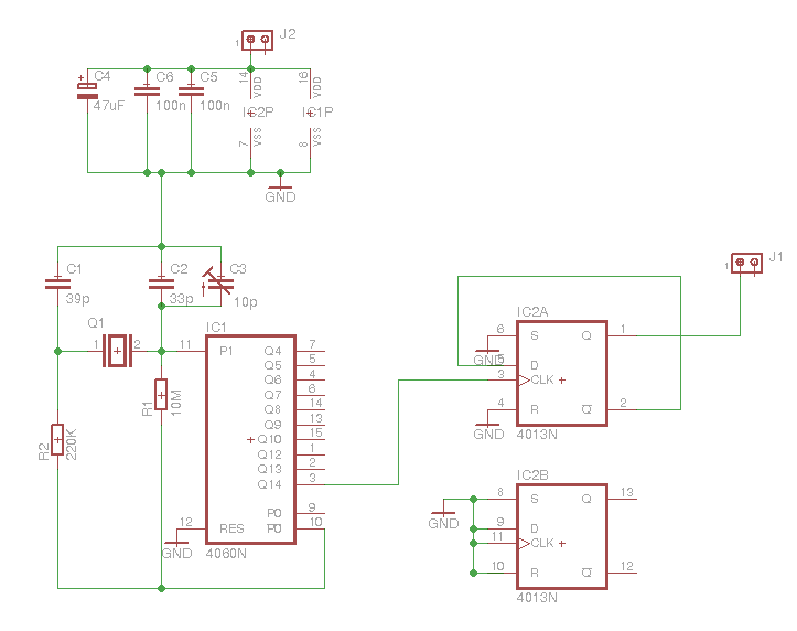
1 Hz clock generator
The 1 Hz generator based on a 32 kHz watch Xtal. J1 goes to the (ex-)Arduino
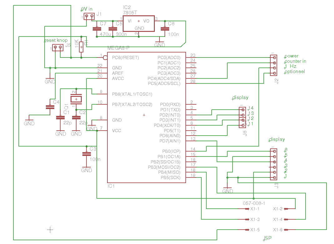
Atmel ATmega328 from an Arduino
The Atmel from an Arduino. Programmed with bootloader and placed on a pcb.
Prescaler
The prescaler schematic.
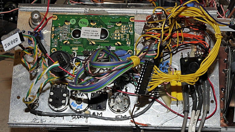
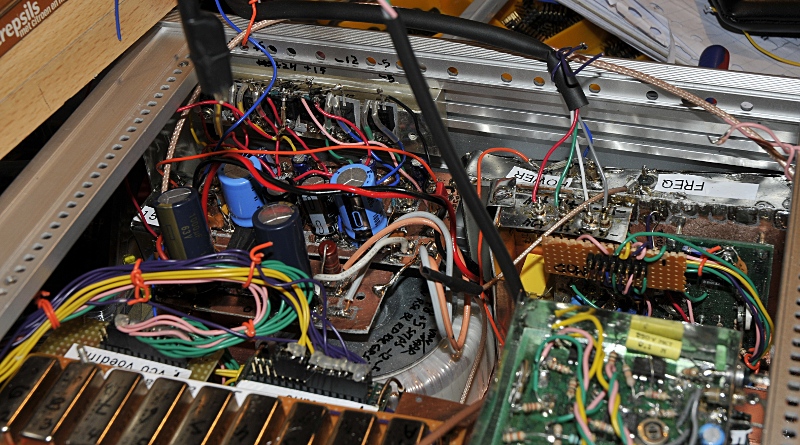
At the end the PSU did not fit the cabinet. Some relais pins were broken because off the fiddeling to get it in the cabinet. It was a real ratsnest with wires and I could not reach any module to adjust or repair. I forgot to connect the relaisboard but that the connection had to be soldered on the bottomsite that I could not reach. So I took everything out again and made headers to all modules. Made some interconnect cables and routed all PSU wires to one place. The same for the front. Now all potentiometers have a connector and label.
From the top with the new VCO relais board
From the backsite with room for the mainsfilter entrance
View from the frontside
The frontpanel
The powerrails. The cabinet is the heatsinck
And then it is finnished. While doing the final tests I found a few small things to solve or improve but the result is allready very usable.
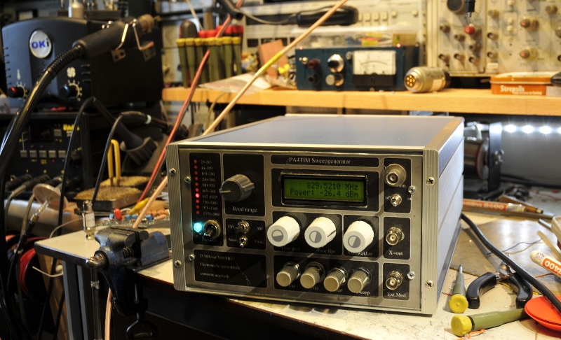
Finnished in its enclosure