This is a full featured but broken Tek spectrum analyser. It has the tracking generator, 300Hz filter, high res counter and video option installed. It was a gift from a circuits online member who did not had any use for it, and had no time to repair it. Thanks Gori.
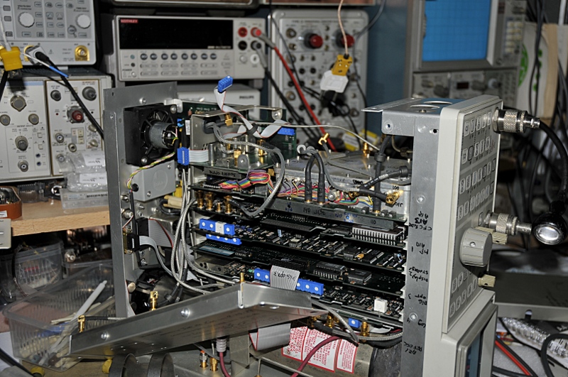
It seems to do something, all buttons react, i see a trace and it boots up. But the read out is a blur and there is a raster of dots on the display. All coax-patchcables were not connected, so first some puzzling to make all the right connections before powering up. A first inspection of the PSU rails showed some very dirty signals , wobbling voltages and rather big ripples. So first job, remove the psu board and check caps. I rather do the checking by measuring with a probes under power but it is very hard to find the caps from the bottom side and the topside is covered with the rest of the SA. It is a bit stuffed so to say.
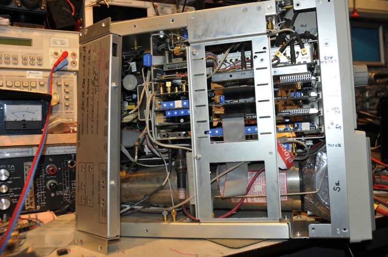
Vieuw from the bottom with PSU and sweep print
The L shaped board is the psu board. If you measure with a scope on the right top corner part, you need a diff probe or isolation transformer. This is a switched mode power supply. It is a very complex PSU. There are 2 pwm controllers that you have to synchronize .
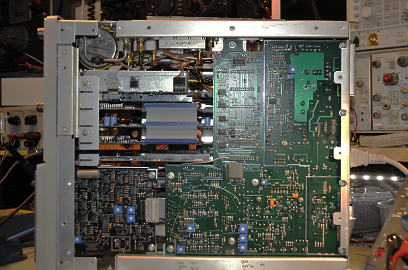
The front and bottom
The top side with the VR box pulled aside
First the board retainer has to go, all plugin boards under it and a bunch of connectors.
To be continued…
The display looks like this, I forgot to make a picture from mine (photo from http://www.edaboard.com/thread158959.html )
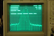
Display problem
Service manual: tek_2710_svc
I changed all electrolytic caps. A few turned out to be allready replacements and one was soldered with the polarity wrong. Most had a to high DF. Two in the PSU were real bad.
Powering up without an isolation transformer caused an earth leakage. The caps between earth and phase/zero turned out to be good there was no DC leakage, so there must be a leaking cap in the second filter.
This is a late 2710 and the manual is not very helpful, schematics are hard to read and the text about adjusting are for the first version. The 2712 manual is downloadable at the site of KO4BB. The procedures in there for the later model 2710 are very usefull for the 2710. for instance the way to sync the preregulator of the second switcher and adjusting the voltages.
There is a trace, it reacts on menus but the readout is unreadable (hmm, so it is now an unreadout 🙂 ) . Sawtooth is OK. Charcters are written through vectors. So something seems to go wrong with the character generation or the vector writing
At this moment I have a stable powersupply if I turn off the read out. With readout the supplys wobbles about 200 mV up and down. So something is pulling the PSU down. We will see, first the netfilter. Most important thing is always first getting the PSU perfect.
Update:
The netfilter should have 3 caps and a common mode choke. I measured 2 x 12 pF and 8 nF so that should mean two caps are shot. I already noticed there was DC leakage, but two dead Y caps is not good so I placed new ones. I opened the old one and to my surprise there only was a X cap. So not according the schematic. This means the leak must be somewhere else. So I had to remove the @#$% thing again (no fun).
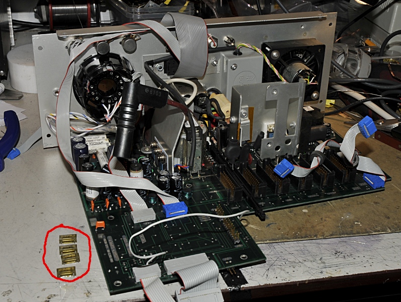
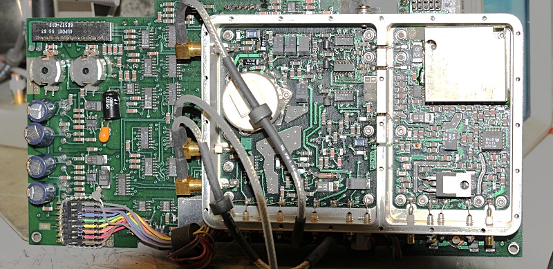
PSU board
In the red circle you see 4 caps that showed 10-25 uA leakage at 350VDC, besides that the housing was cracked. Replacing them is not easy. You have to remover the backpanel for acces. No sign of this 2n2 caps in the schematic. They are bet
ween hot and ground and neutral and ground. 40 uA is enough to trip the earth-leak detector and these 4 together go easy over that value.
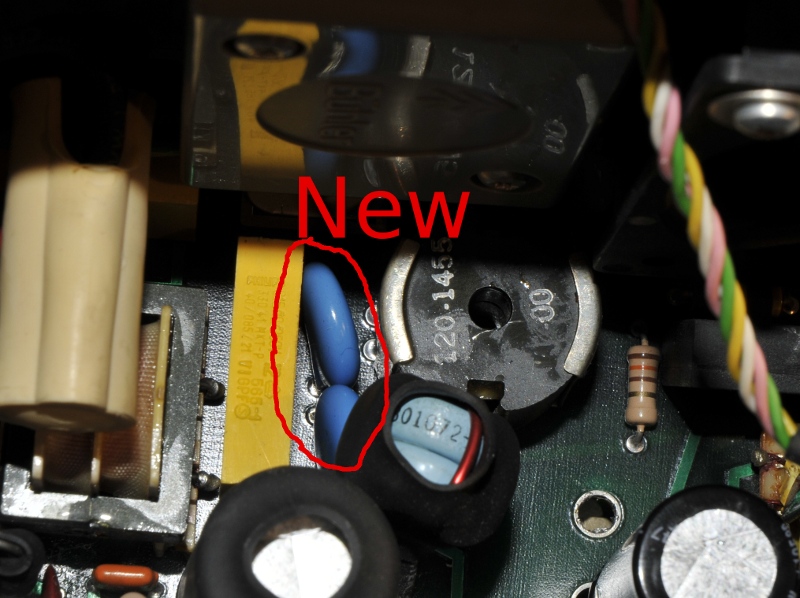
two of the new Y caps
The blue caps are the replacement. The yellow are MKP X caps and tested still good.
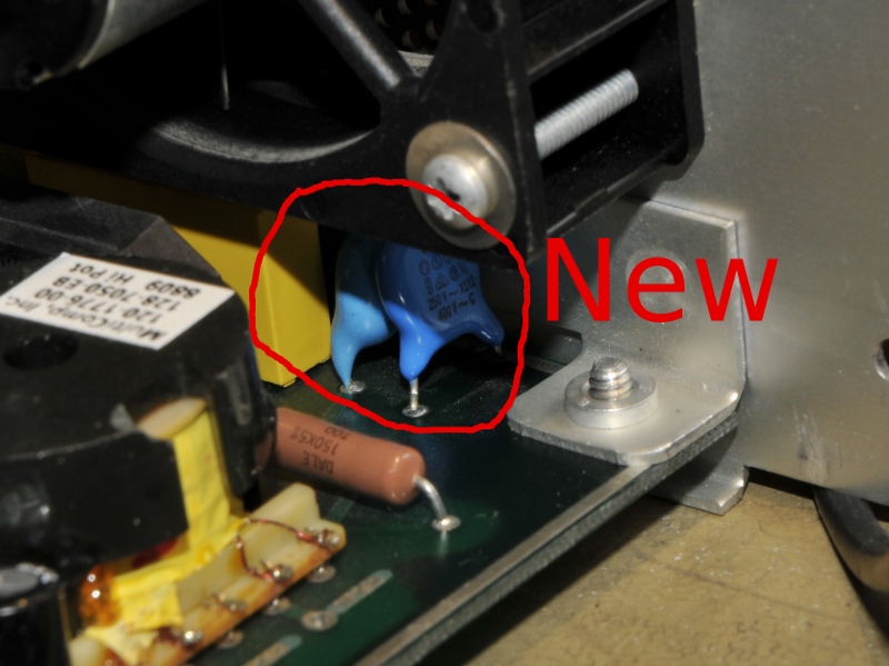
Second pair
Here you see the problem of space.
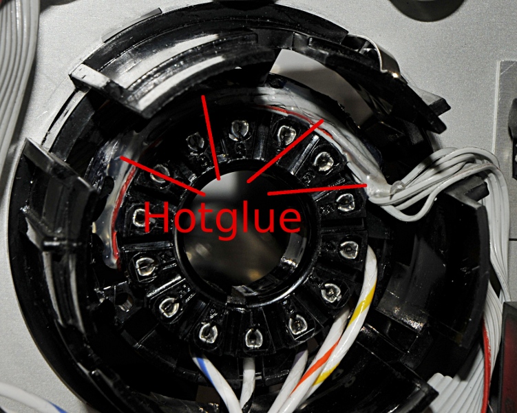
CRT connector mod
The crt connector is made of two separate parts. The ring in the chassis and the connector. It has a bunch of wires and they are thin. It costed me 10 minutes last time to guide them so they did not get crushed by the crt pins. I now hotglued them in place. Not to much glue in case it would melt through the heat of the CRT. Just enough to mount it with more ease.
Update 8-8-13:
U146, a PLS159 looks to be dead on pin 19. There is 1,75V there. But that is low for pin 1/2 of the U204 that is behind it. Pin 13 is pulsing so output 12 should react. Even static it stayed in the wrong state. So I replaced U204. Now the squared changed into stripes. Stil no activity on the output. Then I took a resistor and pulled pin 1/2 to ground. I expected to see some reaction on the screen like parts of characters but to my suprise I now have a perfect working read out. It looks like the display update of the read out is now a bit lagging but at least I can see error messages and read menus.
After booting I got 99 errors about some files. It asked to proceed and I said yes, then it asked to fix the file system and it did. Now it starts without a single error. Then I normalised, that took a while and only gave a frequency cal error. Not so strange because I still have no signal. The 100 MHz reference oscilator is OK, the attenuator too.
Now I have to measure the first converter. But first change all the tantalum caps. Many are a bit disformed and some show cracks, onder the microscope. While removing one for measurement it popped and its guts came out. Others all had very high ESR and leaked to much current. Replaced some critical ones already but today the new ordered once arrived. Quick measurements on the mosfet driver show that the YIG (first LO) should have to work, at least the FM part. I can change frequency too so the main YIG looks to be OK. This is not easy, all modules are coupled with semi rigid coax through SMA and hard to reach. To be continued…
Read out working
The readout is working, many tests succeed, The display was off centre. That was caused by a broken wire between horizontal position and PCB A15 J2. Now it centres well.
But everything todo with frequency normalisation fails. So upto the first converter..
Update:
The error ‘main DAC frequency error’ and scope measurents with a HP 500-3000 MHz downconveter brought me to the YIG. It was kinda running but distorted and off frequency. The TG worked fine, did some other tests and I followed the signal upto the 400 MHz filter. I think at this moment the problem is in the YIG or the control. I was hoping for an analog problem instead of a dead DAC so I decided to take a look at the YIG.
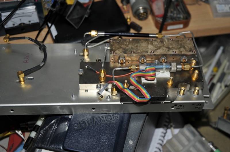
RF motherboard
The problem is this thing is tucked away rather deep. First you have to remove the RF unit. That is a lot of work and you need to be very carefull. The YIG is mounted to the unit. A YIG is an oscillator driven by two coils. The 1st LO interface is mounted on top.
Down here you see it, it is housed in an inox cup. There are three trimmers inside. They are sealed. I’m not planning to adjust them but just in case it should be needed I drilled 3 holes in the cup. parallel to one of the coils are two 820 uF capacitors. I desoldered them for testing because a shorted one could cause the psu instability related to the sweep. Both had a high DF and lost about half the capacitance. Then I tested them for leakage and one of the two went well upto about 3 a 4 V and then shorted massive with a 0,5V voltdrop. So I replaced both. The new black ones are low ESR panasonics but a bit bigger. So it needed some puzzling to fit them. Next step is testing the two orange tantalums that are famous for causing problems. They have many advantages but can not handel over voltage. And damage very easy, then nasty things like thermal runnaway can happen and they can blow up. Failure if they do not blow is forming a short. If used the right way they should be able to run for ever.
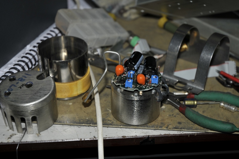
YIG
And below are the “sad” remainders. I hope the rebuilding is less hard as taking it apart.
Operation to remove YIG
The tantalums turned out to be bad too. One was leaking to much, the other had a D of 0,4 and that is to high.
Now the RF board is out I first check the filters with my vna.
I bought a service manual from http://artekmanuals.com/ . Very good quality scans voor a very fair prices. He did not have a pdf for my version but had a paper one and scanned one within a few days.
Update:
Removed the lid of the LF and HFVCO. Replaced a dead 74LS00. U510 on the LF board. This was giving sawtoothlike outputs and runts. Just to be shure I replaced it. Now the signals are nice and clean. For the rest I could not find strange things. Turning C511 gives errors about beatnote when you go to low or to high. Beat is connector J540.
CFC board with a defectig IC. Allready replaced here.
But still no 10MHz IF so that will be the next very difficult step. The RF motherboard 2nd converter is covered by a soldered shield. There are some test point. The jumpers disconnect the 110MHz, and there is a 110MHz test connector “hidden” under the deck. But for serious trouble shooting I have to find a way to open it. At this moment I think the 110-100MHz to 10 MHz mixer is dead.
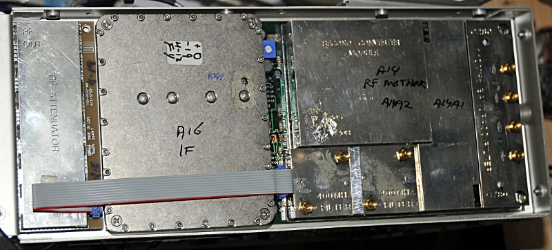
The RF motherboard and 1st converter. The YIG is most left on the other side
I made a picture that I combined with the SM component picture
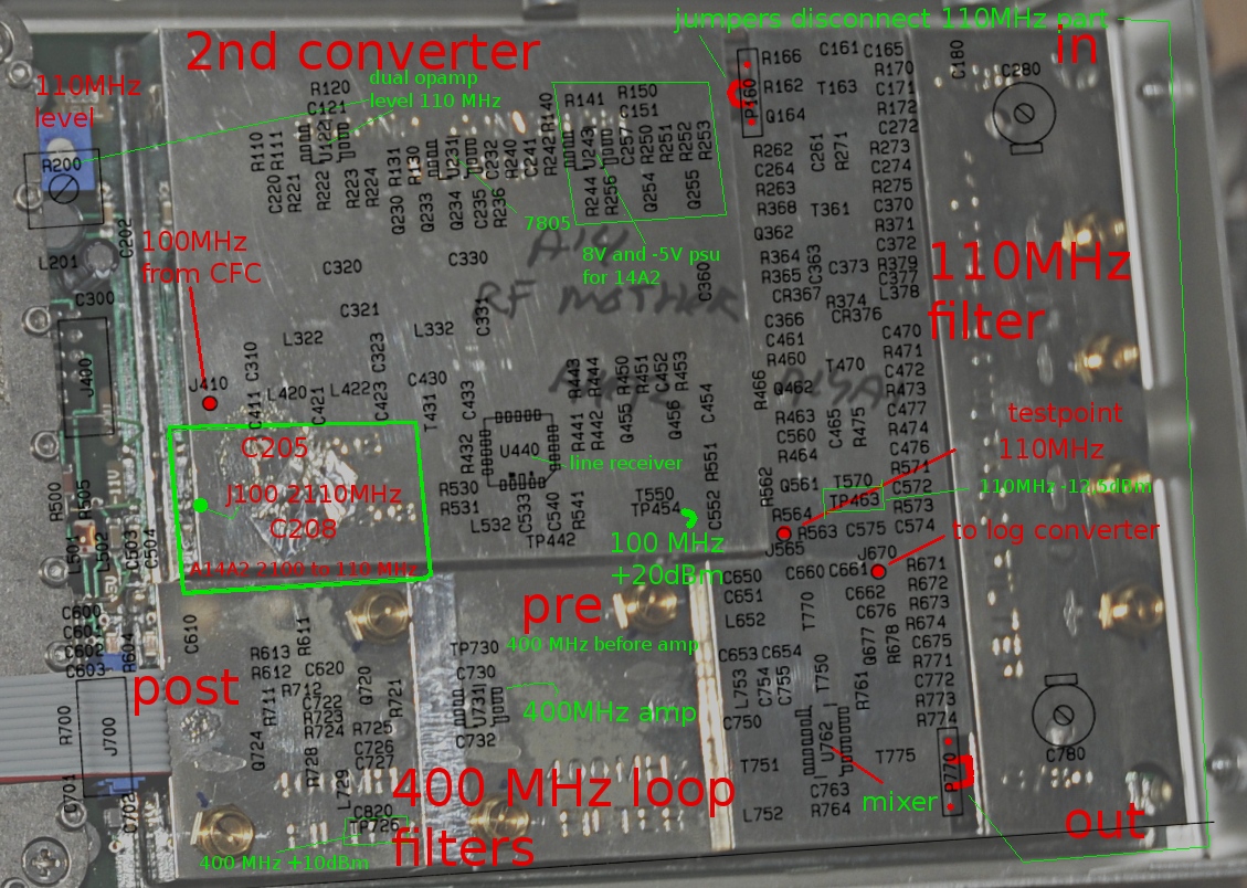
A14A1 and A14A2 2nd converter
Update:
Because I lost signal in the 2nd converter I had no choise other then removing the shielding. I decided to use a modded paintstripper http://www.pa4tim.nl/?p=4598 to heat it. In about 20 seconds I could take it off.
There are two pcbs inside and they are soldered all around. I’m afraid that getting it totally closed again, will be harder .
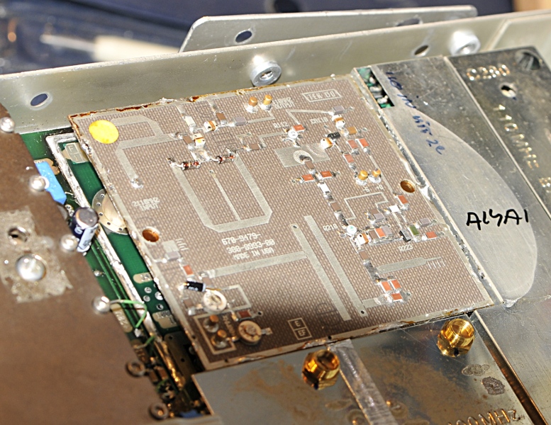
2nd and 3th converter without shield
Now I was able to measure the signals and make some adjustments. The result was a pleasant surprise. Finally a trace. It still does not pass the normalization, but now I can adjust everything while monitoring the result. It also shows external signals, so the analog part is OK and the digistuff seems to do it’s job. The VCO locks, reading is OK, markers work, so that is a good start. Now I’m doing every step of the adjustment chapter.
finally, a trace
Update:
Still not able to normalize and the amplitude was way to low. In some bandwidths there was no signal at all. The problems were caused by the filters in the VR unit. There is a 500 kHz, 30 kHz and 3 kHz filter and after peaking those the amplitude is now right. So the only problem left is the normalisation. But now amplitude is good and everything seems to work, I will first do all the alignment steps from the manual. Problem about the HFVCO is that the firmware leads you trough that. It tells you that you need to measure a voltage on a feedtrough capacitor at the bottom. But it does not tell wich one. The feedtroughs that are available do not have a relation to the vco. Three are used for digital and the rest is from the powersupply. But the normalisation error is related to the HFVCO. So I have to study the schematic first.
Update:
Finaly, frequency normalisation without errors. I’m happy. But still a lot to do. The log amp is not linear enough. But maybe that adjustment still comes. Most important part is it does not give error messages anymore. So I leave the HFVCO as it is right now. No errors, so I have probably set it right.
Update, 30-8-2012
It passed every test, all adjustments are done and it is ready for use, pfffff, what a job this was.
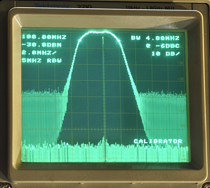
Alignment of the shape of one of the filters.
Aligning the filters was very much work. The one above was almost 2 MHz off. Here the shape is nice but it is still a bit to low. But after adjustment of the LO it was perfect.
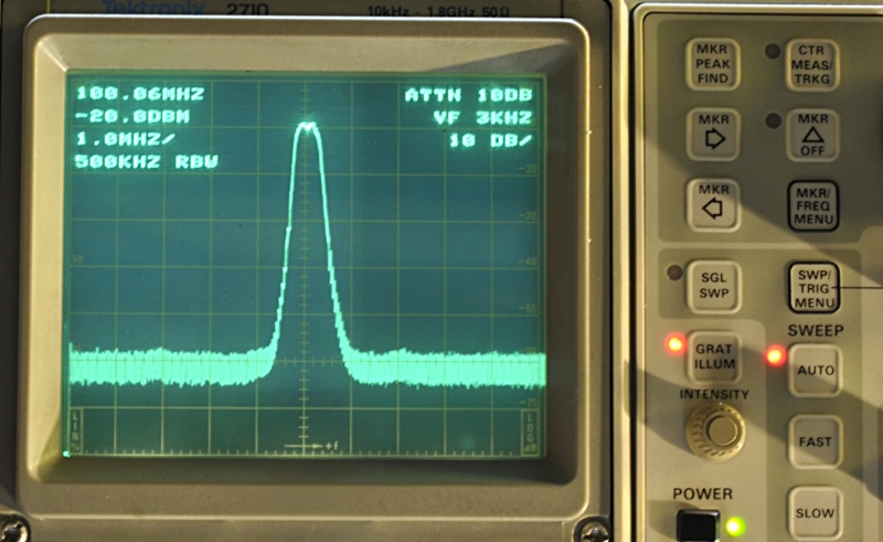
And here the first measurement after it was finnished.
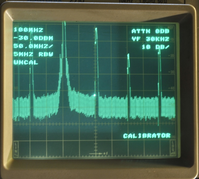
Ready for use. My 100MHz standard
Testing the 1602 susceptance standard with a SA
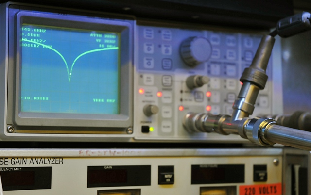
The tracking generator in action.
Repair of this SA took me a few months. There seem to be a lot of dead 2710’s around but you seldom hear about a dead 2712. I have the latter too. I prefer the 2712 over the 2710. It is more ergonomic and has normal keys instead of the industrial type switches under foil. Performance is the same. The 2710 was made primarily for field use.
Update:
Many people mail me because their 2710 is dead. I do not have this SA anymore, I gave it to a friend who used it a few years until it died again. I would love to help everybody but I just do not have the time and this thing is very complicated so diving again in the books costs to much time. I hope you understand.
Here an update from Graham who gave some very usefull information that could be of some help:
My screen also has gone into the dreaded displaying garbage symptoms.
After spending a lot of frustrating time playing around i think i can
put my finger on the problem (mine anyway), digital is certainly not
one of my strong points but here goes..

It seems the SA's display pages are changed by pin 7 of U260 (PLS159),
this chip is supposed to send a negative pulse to a binary counter
(U326). The binary counter counts until the correct page/s is
displayed then is suppose to stop.
The binary counter also sends signals to other chips including U308
which controls blanking and "dotenable"! (one of the classic things we
all see with the fault)...
What seems to be happening (in mine anyway) is that U260's pin 7 is
caught in a near mid state, around 4V in mine- any noise in the
circuit is +- on the 4v and sending the page select counter into near
constant counting- this seems to be why we see all of these unusual
displays....

Now to prove the point, i pulled the pin 7 output up to 5v with a high
value resistor- the SA now always boots to a spectrum display which i
assume must be default with the initial (000?) binary output from the
counter.. no other screen data is displayed but at least i can see a
working spectrum..
I experimented with mosfet switching on pin7 to lighten its load but
had no success.. I dont think it pulls down at all...

Now all i have to do is find a PLS159, the code and try to program it!
GEEZ!! (id very very thankful if one of you guys can help)
I dont think the PLS is doing very much looking at its clock, but for
me the code would be very difficult to invent..

Hope i have been of help.